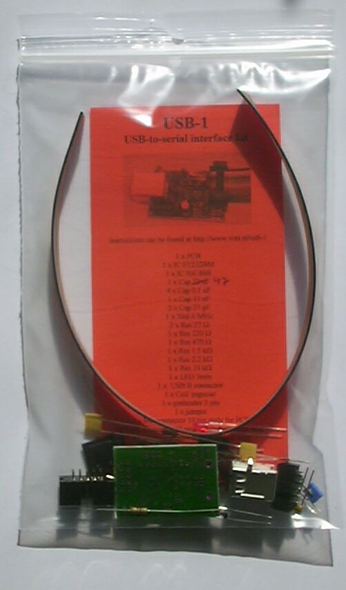
USB-1 : USB-to-serial interface kit
|
|
USB-1 : USB-to-serial interface kit |
|
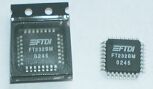
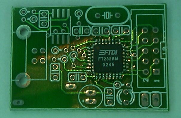
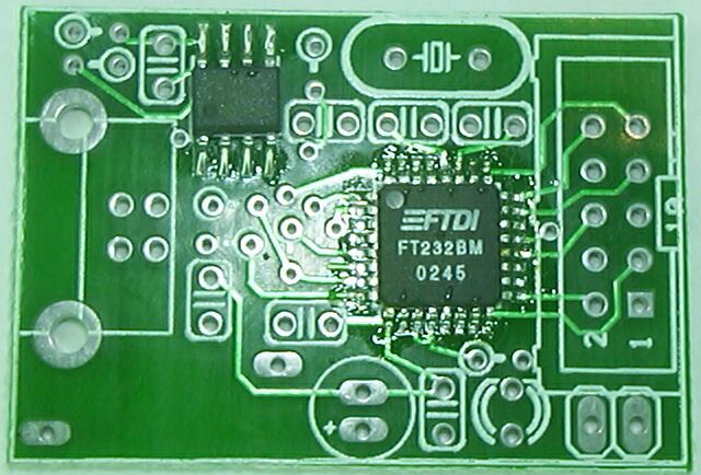
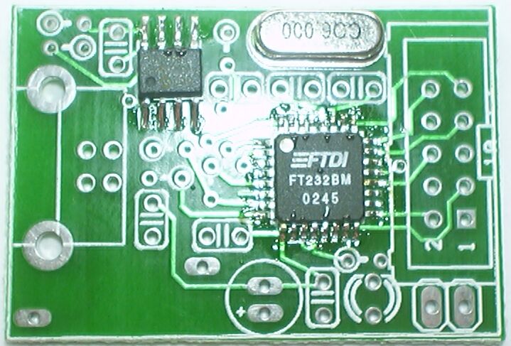
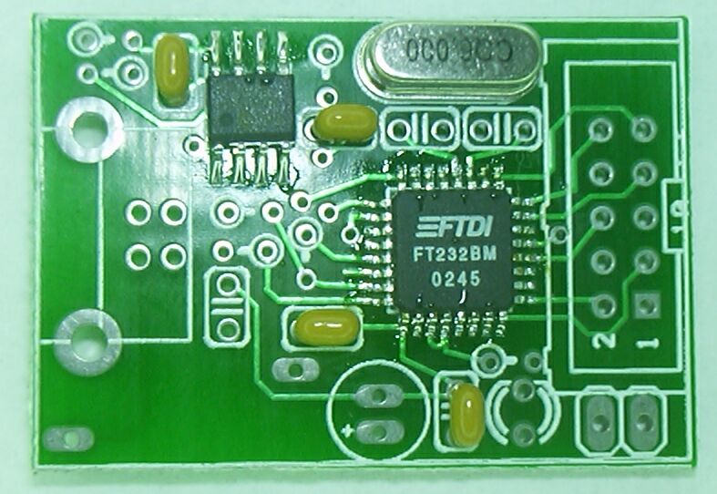
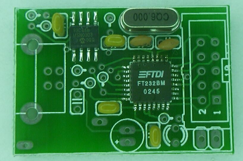
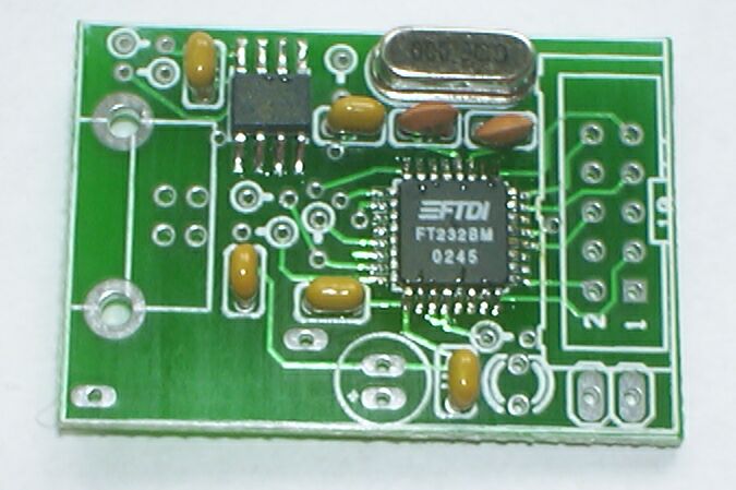
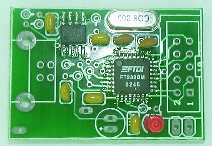
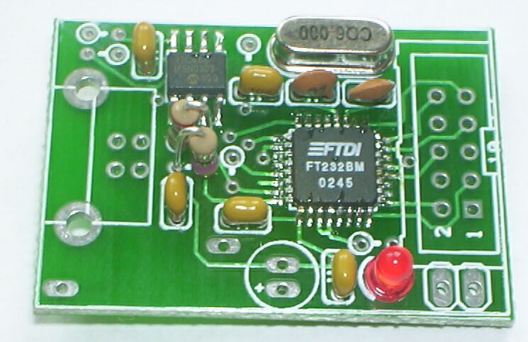
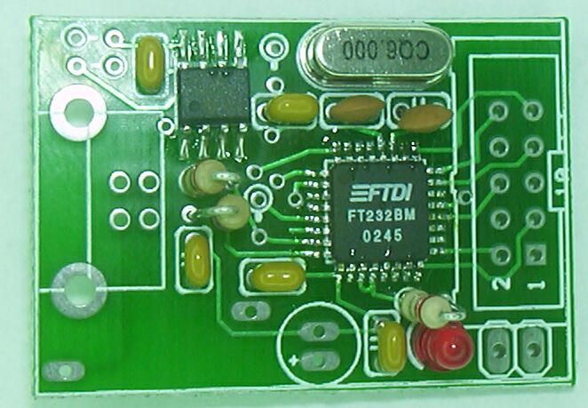
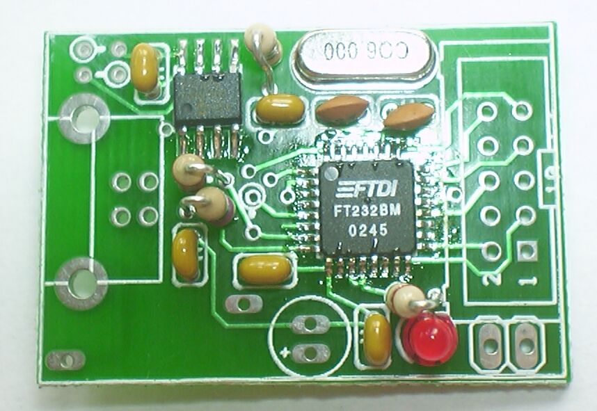
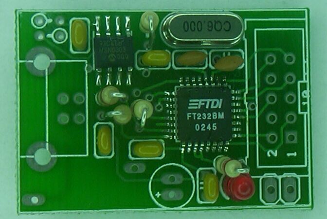
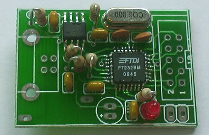
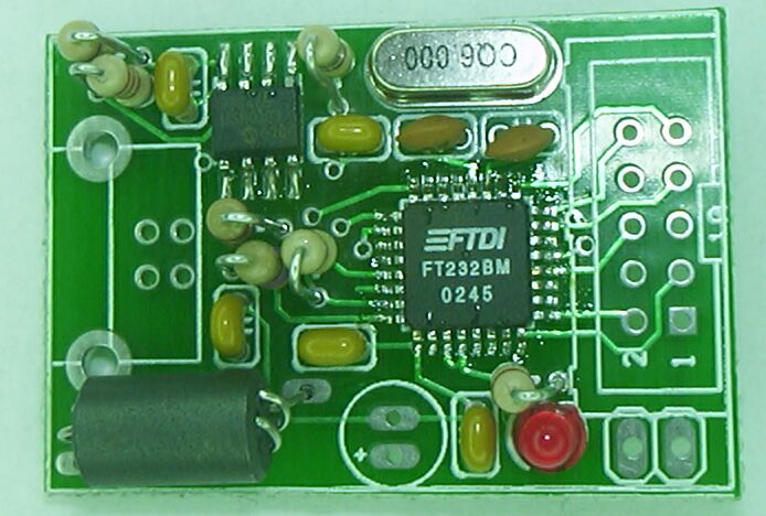
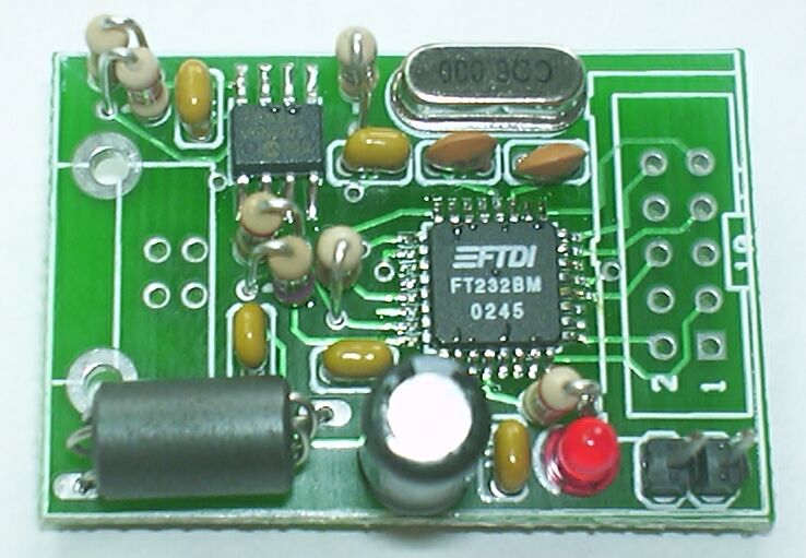
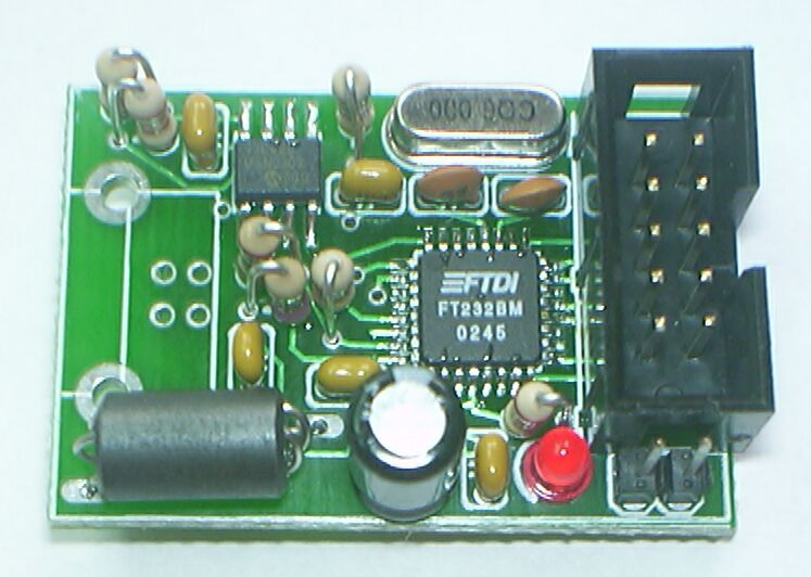
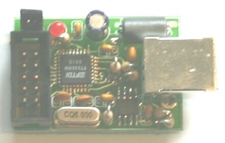
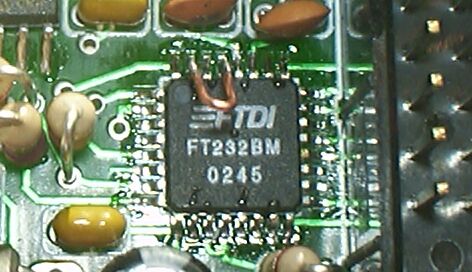
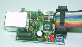
PurposeThe USB-1 is a complete USB interface. It can be connected directly to a microcontroller, or you can add a MAX232 chip to create an interface at RS-232 voltage level and polarity. USB-1 uses the FT232BM chip. The manufacturer of this chip supplies drivers that can be used to create a virtual communication port on your host PC, so you don't need to write any special software. Just use the port as you would use any normal serial port. This kit uses two SMD ICs, one of which has 32 very small legs. This is definitely not a beginners kit. Circuit
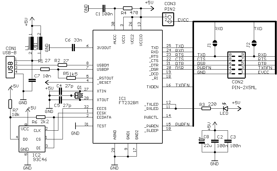
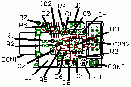
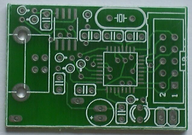
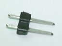
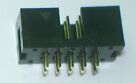
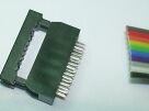
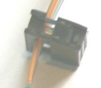
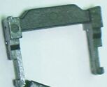
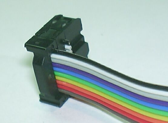
The circuit is the standard FT232BM circuit, refer to the FT232BM datasheet for a discussion of the various aspects. CON-3 is a two pin header that can be bridged by a jumper to provide the USB power to pin 1 of CON-2. This can be used to power a bus-powered device, but you will need an additional circuitry to switch the power to comply to the USB rules. Refer to the FT232BM datasheet and design notes for information. When the circuit that you want to attach has its own power it is best to leave out the jumper, or to leave pin 1 of CON-2 unconnected. The PCB designed to accomodate an ML10 header as CON-2, but you can substitute any other standard connector, or directly connect wires. The kit contains the male ML10 header, and a strip of 10-wire colored ribbon cable, with a matching crimp-on female ML10 connector. Use it or as you see fit. For the most simple use you need only three pins of CON-2: GND (2), RXD (10) and TXD (9). You might want to provide handshake back to your PC application by connecting RTS (7) to CTS (8), and DTR (5) to DSR (6). Note that these handshake connection points are conveniently located to be bridged by short pieces of wire. The pinout of CON-3 matches the UART connections of port C of a Dwarf Board micrcontroller board with an 28-pin PICmicro. AssemblyI assume you know how to solder a PCB, otherwise this is definitely not a kit for you. You will need a good soldering iron, a steady hand and most important: a good magnifying glass to check your work. A piece of thin solder and a piece of desoldering braid are supplied with the kit. The most difficult component to solder is the FT232BM chip itself. There are basically two approaches to soldering an SMD chip like this: get it right the first time, or removing excess solder with desoldering braid. With my much-too-broad tip I can manage to get most of the pins right, using the braid for the one or two pins at each side that got too much solder. With a finer tip you might succeed to get all pins right. When the tip of your iron is (too) big (like mine) the best tip I can give you is to use remove excess solder from the tip before using it, and to use as little solder as possible. This reduces the chance of making bridges. The kit contains some very thin solder, use it. It might seem to be a very short piece for the job, but you should not need more than half of it. Idem for the desoldering braid. You can click on each of the pictures to get a larger picture.
UseThe electrical interface is specified in the table below, with the corresponding wire colors (assuming you assembled the cable and header conform the instructions). In the most common case you will use only pins 2 (ground), 9 (transmit to PC) and 10 (receive from PC).
For PCB version b1.04 (you can find the number on the solder side of the PCB) and lower the TXD and RXD lines were swapped, as shown in the table below. PCB b1.05 and higher can in most cases be connected directly to the appropriate a Dwarf Board bus.
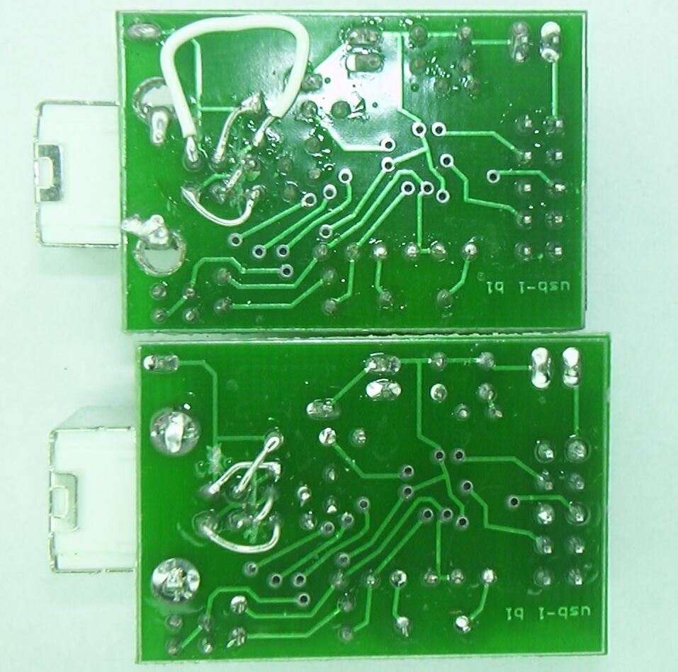
ErrataThe b1 version of the PCB has an error: the USB connector is connected 'backwards'. The picture below shows how this can be corrected by cutting 4 traces and reconnecting in the correct way. This version of the PCB was used for ty-outs, it has not been part of purchased kits.
The b1.02 and b1.03 versions of the PCB have an omission: pin 31 of the FT232BM (test) should be connected to ground (as shown in the circuit diagram), but on the PCB this pin is not connected. So use a small wire to make a connection between pin 31 and pin 29 (which is connected to ground).
The b1.04 PCB does not need any special handling, but the previous version of this page showed the wrong way to assemble the crimp connector, which resulted in a mirrored connection. The current page shows the correct way. The b1.05 PCB does not need any special handling, but note that the RXD and TXD connections have been swapped with respect to version b1.04. Links
http://www.voti.nl/usb-1
| |||||||||||||||||||||||||||||||||||||||||||||||||||||||||||||||||||||||||||||||||||||||||||||||||||||||||||||||||||||||||||||