Introduction
Wisp628 is a FLASH PICmicro controller programmer.
This document describes the assembly of the Wisp628 kit.
Refer to the Wisp628 web page at
http://www.voti.nl/wisp628
for information about the Wisp628 circuit,
the communication protocol, supported PICmicro controllers,
PC software, blink-a-LED programs, FAQ, etc.
Assembly
I assume you know how to solder a PCB.
The Wisp628 PCB contains some fine traces,
but it is not difficult to build for someone with a little experience.
Be patient, don't use too much solder and check your work under a
strong lamp (a magnifying glass might be handy).
When bending the leads of the components before inserting into the PCB
make sure you bend as close to the component as possible.
You can click on each of the pictures to get a larger picture.

|
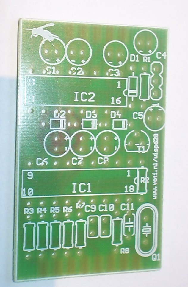
The description assumes that you have the board oriented as shown,
so you can read the component designations on the silkscreen (component) side.
|

|

|
Place the three small 1n4148 diodes D2, D3 and D4.
The dark band points to the right.
Solder the diodes.
|

|

|
Place and solder the two 1 kΩ resistors (brown-black-red) R1 and R2.
|

|

|
Place and solder the six 47 Ω resistors (yellow-purple-black)
R3, R4, R5, R6, R7 and R8.
|

|

|
Place and solder the big 1n4004 diode D1. The white ring must be towards you.
|

|

|
The next two steps are crucial.
The two D connectors are fitted directly over the PCB edge.
Depending on the tolerances of the connectors this fit can
be loose or tight.
In both cases the solder cups must be aligned accurately with the solder pads
before soldering. First fit and solder the male D15
(the one with pins, not the one with holes) at the near side of the board.
The row with the most pins (8) is soldered (on the solder side of the PCB, of course),
the other row (the 7 pins on the component side) is not used.
Do not try to touch the pads while soldering: heat the connector cup and apply
a little solder between the cup and the pad.
|

|

|
The female D9 connector is soldered at the far side.
Take care not to make a short between pins 4 and 5 and the trace near the pads
for these pins.
Due to board size tolerances you might have to keep a little space between
the connector and the board to avoid such a short.
|

|

|
Place and solder the 2n3904 transistor. The middle (base) lead must be bent
somewhat towards the round side.
|

|

|
Place and solder the two smaller 22 pF or 20 pF disk capacitors (C9, C10).
The holes on the PCB are too close for a normal fit.
It is recommended to bent the leads like the right cap on the picture.
|

|


|
Place and solder the 0.1 µF capacitor (C11),
which can be a disk type or a small blue one.
|

|

|
Place and solder the larger of the two IC sockets.
The indent must be at the right side.
|

|

|
Place and solder the smaller of the two IC sockets.
The indent must again be at the right side.
|

|
|
|

|
WARNING: The pictures incorrectly show a 1uF elco for c8 and a 22uF for c4.
The correct placement is: 4 * 1uF elco near the D9 connector and 2 between the chips.
Place and solder the six 1 µF capacitors (C1, C2, C3, C4, C6, C7).
The two in the middle of the PCB (C6, C7) must have the white stripe towards you.
The four at the far (C1, C2, C3, C4) end must have the white strip towards the left.
You might want to straighten the leads first.
|

|

|
Place and solder the two 22 µF capacitors (C5, C8).
The one at the middle right side (C5) has the white strip towards the right,
the one at the left side of the transistor (C8) has the white strip towards you.
|

|

|
Place and solder the crystal.
|

|


|
Insert the two ICs into their sockets.
You might need to bent the pins of the ICs slightly to the middle before inserting.
Take care not to fold a pin under the IC.
Both ICs must be placed with pin one (the pin with the dot) away from you
(the indent to the right).
This finishes the assembly of the PCB.
A place for a three pin header remains unused;
it can be used to connect a 5 Volt power supply
(center pin == +5 Volt, outer pins == ground).
|

|

|
Strip the ends of the colored wires and solder them to the remaining
(female) D15 connector,
as shown: 1 = black, 2 = red, 3 = green, 4 = blue, 5 = yellow, 6 = white.
The connector has the numbers on it. In case your eyes are as bad as mine:
with the connector in front of you, largest row up, solder cups towards you,
pin 1 is the upper left.
|

|

|
Assemble the connector.
The clamp can be used when you put it together with both curves in the same
direction (for a thicker cable you would have both curves in opposite direction).
|

|

|